
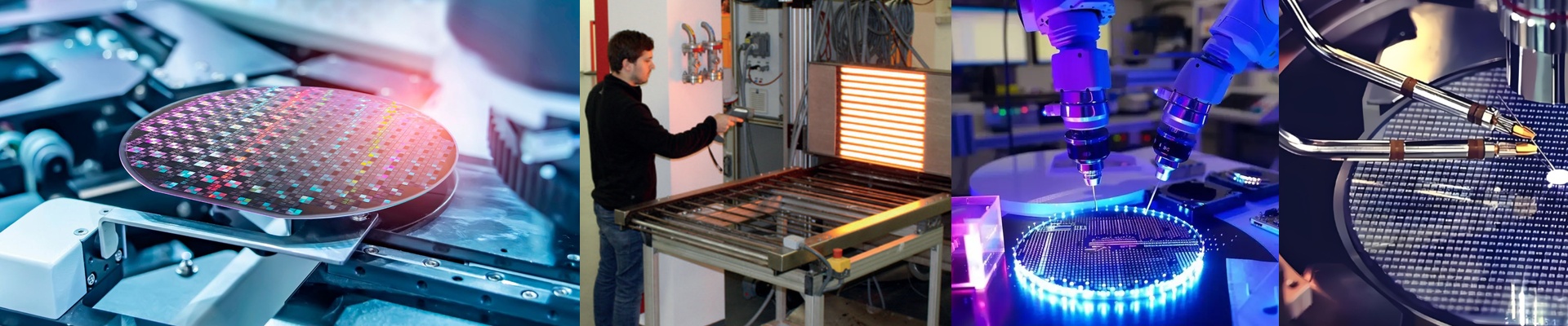
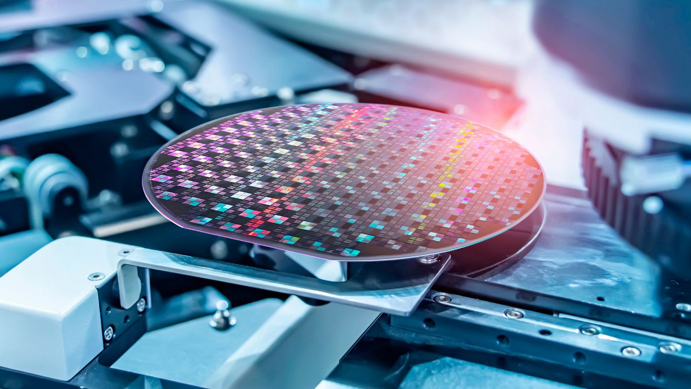
On the fab floor, a 1°C drift during the photoresist bake isn’t just a blip on the monitor. It shows up as linewidth variation, etch bias, and scrap wafers. We built our semiconductor infrared heating lamps to take that variability out of the thermal budget. What matters technically We run short-wave infrared emitters, dumping heat directly into the wafer and substrate with rapid, direct-coupled transfer. You get sub-second response and wafer-level uniformity within ±0.1°C across the bake surface. That kind of precision shows up as tighter critical dimension control in lithography and consistent profiles after etch. The system is cleanroom-ready, compatible with Class 1–100 environments, and engineered to hold particle counts at zero during steady-state operation. Output stays stable over 5,000+ hours with less than 5% intensity drift, so you can run 24/7 with minimal scheduled maintenance. Why it works where we need it In photoresist processing, the soft bake and hard bake steps set solvent removal and polymer crosslinking. With our lamps, the temperature profile across the wafer is repeatable, so you see consistent adhesion, fewer defects, and predictable CD performance after exposure and etch. The fast thermal cycle also cuts chamber turnaround, boosting tool throughput without pushing energy draw higher. In production, that translates to fewer rework lots, stable yield, and a lower operating cost per wafer. The practical details The lamps are compact and modular, but alignment to the wafer plane is critical. Expect tight focus on emitter-to-substrate distance, and make sure you have tool-side interlocks and temperature feedback loops in place. Integration is straightforward on most tracks and bake plates, though thermal mass shifts with chuck design. Run a short qualification to lock the recipe before you roll it out.